

축적 및 개발 20 년 이상 후, 우리 회사는 기술 혁신과 인재 풀에 분명한 이점이 있습니다. 앞으로는 고객에게 더 나은 제품과 서비스를 제공하기 위해 실제 조치의 속도를 높여야합니다.
의사 짱 -하문 powerway 첨단 재료 공동의 CEO., LTD


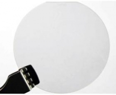
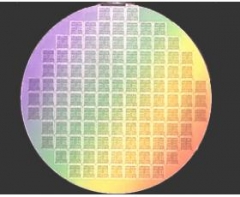
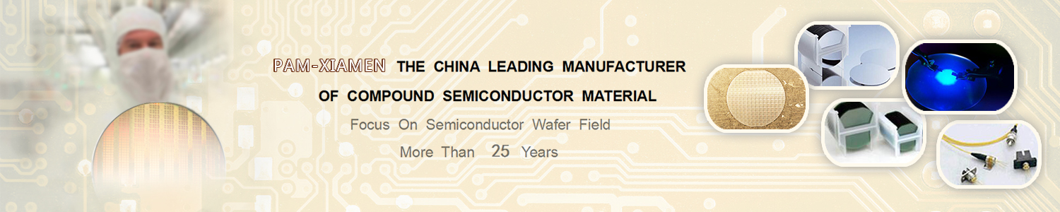
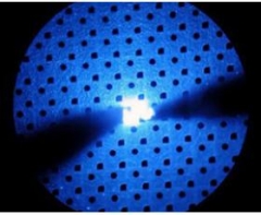
pwam은 화합물 반도체 기판 인 갈륨 아세 나이드 결정체와 웨이퍼를 개발 및 제조합니다. 우리는 첨단 결정 성장 기술, 수직 구배 동결 (vgf) 및 가우스 웨이퍼 처리 기술을 사용하고 있으며, 결정 성장, 절단, 연삭에서 연마 가공 및 웨이퍼 청소 및 포장을위한 100 가지 클린 룸. 우리의 gaas 웨이퍼는 led, ld 및 microelectronics 응용 분야에 2 ~ 6 인치 주괴 / 웨이퍼를 포함합니다. 우리는 항상 현재 하위 상태의 품질을 개선하고 대형 기판을 개발하기 위해 노력하고 있습니다.12
pam-xiamen의 gan (질화 갈륨) 기반의 에피 택셜 웨이퍼는 초고 휘도의 청색 및 녹색 발광 다이오드 (LED) 및 레이저 다이오드 (LD) 애플리케이션 용입니다.
갈륨 질화물 (gan) hemts (높은 전자 이동성 트랜지스터)는 rf 전력 트랜지스터 기술의 차세대 기술입니다. 팸 - 샤먼은 현재 사파이어 또는 실리콘에 algan / gan hemt epi 웨이퍼를 제공하고 사파이어 템플릿에는 algan / gan을 제공합니다 .


문의를 통해 무료 서비스를받을 수 있습니다. 25 개 이상의 경험 반도체 라인.

우리의 목표는 모든 요구 사항을 충족시키는 것입니다. 아무리 작은 주문이라도 과 얼마나 어려운 질문 자격을 갖춘 제품과 만족스러운 서비스를 통해 모든 고객에 대해 지속적이고 수익성있는 성장을 유지할 수 있습니다.

~ 이상 25 년 이상 경험담 화합물 반도체 소재 분야 및 수출 사업에서 우리 팀은 고객의 요구 사항을 이해하고 전문적으로 프로젝트를 처리 할 수 있음을 보증 할 수 있습니다.

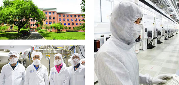
품질이 최우선입니다. 팸 - 시아 먼은 iso9001 : 2008 는 고객의 다양한 니즈를 충족시킬 수있는 상당량의 검증 된 제품을 제공 할 수있는 4 가지 근대적 인 면모를 소유하고 공유하며 모든 주문은 엄격한 품질 시스템을 통해 처리되어야합니다. 테스트 보고서는 각 선적마다 제공되며 각 웨이퍼는 보증 대상입니다.12


Poly -Si 결정은 비용이 저렴하기 때문에 주로 태양 전지에 사용됩니다. 여기서 태양광의 파장에 대한 감도 영역을 확장하여 태양 전지 의 엔지니어링 효율을 높여야 합니다.. Si 또는 Ge 기판 상에 C, Ge(C, Si) 및/또는 Sn 원자로 도핑된 Si(Ge) 막과 같은 IV족 화합물 반도체 막은 이 기술에 대한 잠재적인 솔루션으로 확인되었습니다. 문제. 본 연구에서는 밀도 범함수 이론을 이용하여 Si에서 C, Ge, Sn 원자의 각 원자 구성의 형성 에너지를 계산하였다. Kamiyama et al.이 제안한 "Hakoniwa" 방법. [Materials Science in Semiconductor Processing, 43, 209 (2016)] 비율을 얻기 위해 C, Ge 및/또는 Sn의 최대 3개 원자(최대 4.56%)를 포함하는 Si의 64 원자 슈퍼셀에 적용했습니다. 각 원자 구성 및 Si 밴드갭의 평균값. 기존의 GGA(generalized gradient approximation)뿐만 아니라 screened-exchange local-density approximation(sX-LDA) 기능도 보다 안정적인 Si 밴드갭을 얻기 위해 사용되었습니다. 분석 결과는 네 가지입니다. 첫째, 2개의 C(Sn) 원자는 3일 때 에너지적으로 안정하다.rd , 4 , 6 , 7 , 9 th 는 서로 이웃하는 반면 두 Ge 원자의 안정성은 원자 구성과 무관합니다. 둘째, C와 Ge(Sn) 원자는 2 번째 , 5 번째 , 8 번째 (1 번째 와 8 번째) 일 때 안정하다.) 이웃하는 반면 Sn 및 Ge 원자의 안정성은 원자 구성과 무관합니다. 셋째, Si 밴드갭은 Si가 C 및/또는 Sn 원자(Ge 원자)를 포함할 때 원자 구성에 의존합니다(의존하지 않음). 균일하게 C를 최대 4.68%까지, Ge(Sn)를 최대 3.12%까지 균일하게 도핑하면 Si 밴드갭의 평균값이 감소했습니다. C 도핑은 Si 밴드갭을 가장 많이 감소시켰고 Ge 도핑은 가장 적게 감소시켰...
더 읽기황화암모늄(NH4)2S 처리를 사용한 GaAs 의 웨이퍼 결합은 다양한 구조에 대해 조사되었습니다. n-GaAs/n-GaAs 웨이퍼 결합 구조를 사용하는 III-V 태양 전지 장치의 전기 전도도 에 대한 웨이퍼 오프컷 각도의 영향을 연구합니다. 결합된 샘플의 잘못된 방향을 확인하기 위해 고해상도 x-선 회절이 사용됩니다. 또한 GaAs에서 에피택셜로 성장한 pn 접합의 전기적 특성을 n-GaAs/p-GaAs 웨이퍼 결합 구조와 비교합니다. 고해상도 투과 전자 현미경(HRTEM) 및 주사 투과 전자 현미경(STEM)은 600{도 기호}C RTP 이후 상대적인 잘못된 방향 범위에 걸쳐 인터페이스 형태를 비교하는 데 사용됩니다. 비정질 산화물 개재물에 대한 잘 결합된 결정 영역의 비율은 모든 결합된 샘플에서 일관되며, 이는 잘못된 방향 정도가 고온에서 계면 재결정화 수준에 영향을 미치지 않음을 나타냅니다. 출처:IOP과학 자세한 내용은 당사 웹사이트 www.semiconductorwafers.net을 방문하십시오 . sales@powerwaywafer.com 또는 powerwaymaterial@gmail.com 으로 이메일을 보내주십시오....
더 읽기p 형 6H-SiC 로부터 제조된 다공성 SiC의 광투과도, 광발광(PL)의 온도 의존성 및 라만 산란을 벌크 p 형 6H-SiC 로부터의 것과 비교하였다. . 실온에서 벌크 SiC의 전송 스펙트럼은 3.03eV에서 밴드 갭에 해당하는 상대적으로 날카로운 모서리를 나타내지만 다공성 SiC(PSC)의 전송 가장자리는 밴드 갭을 결정하기에는 너무 넓습니다. 이 넓은 가장자리는 PSC의 표면 상태로 인한 것일 수 있습니다. 실온에서 PSC의 PL은 벌크 SiC의 PL보다 20배 더 강합니다. PL PSC 스펙트럼은 기본적으로 온도와 무관합니다. PSC의 라만 산란 피크의 상대적 강도는 로컬 순서가 상당히 무작위임을 시사하는 벌크 SiC의 것과는 대조적으로 편광 구성과 대체로 독립적입니다. 출처:IOP과학 자세한 내용은 당사 웹사이트 www.semiconductorwafers.net을 방문하십시오 . sales@powerwaywafer.com 또는 powerwaymaterial@gmail.com 으로 이메일을 보내주십시오. ...
더 읽기p 형 6H-SiC 로부터 제조된 다공성 SiC의 광투과도, 광발광(PL)의 온도 의존성 및 라만 산란을 벌크 p 형 6H-SiC 로부터의 것과 비교하였다. . 실온에서 벌크 SiC의 전송 스펙트럼은 3.03eV에서 밴드 갭에 해당하는 상대적으로 날카로운 모서리를 나타내지만 다공성 SiC(PSC)의 전송 가장자리는 밴드 갭을 결정하기에는 너무 넓습니다. 이 넓은 가장자리는 PSC의 표면 상태로 인한 것일 수 있습니다. 실온에서 PSC의 PL은 벌크 SiC의 PL보다 20배 더 강합니다. PL PSC 스펙트럼은 기본적으로 온도와 무관합니다. PSC의 라만 산란 피크의 상대적 강도는 로컬 순서가 상당히 무작위임을 시사하는 벌크 SiC의 것과는 대조적으로 편광 구성과 대체로 독립적입니다. 출처:IOP과학 자세한 내용은 당사 웹사이트 www.semiconductorwafers.net을 방문하십시오 . sales@powerwaywafer.com 또는 powerwaymaterial@gmail.com 으로 이메일을 보내주십시오. ...
더 읽기CdZnTe 결정 의 어닐링 방법은 이 문서에 설명되어 있습니다. 순수한 Cd 및 Zn 금속은 특정 온도에서 CdZnTe에 대한 정확한 Cd 및 Zn 평형 분압을 동시에 제공하는 어닐링 소스로 사용됩니다. 특성화는 균질성이 크게 향상되고 결함 밀도가 1차 이상 감소하여 CdZnTe 결정의 구조적, 광학적 및 전기적 특성이 분명히 이 어닐링에 의해 개선됨을 나타냅니다. 어닐링 후 CdZnTe 품질의 온도 의존성을 조사하면 1073K가 CdZnTe에 대한 바람직한 어닐링 온도임을 알 수 있습니다. 이 어닐링 프로세스는 이미 Cd 1- y Zn 을 사용하여 대략적인 평형 분압 어닐링보다 우수한 것으로 입증되었습니다. 어닐링 소스로 y 합금. 출처:IOP과학 자세한 내용은 당사 웹사이트 www.semiconductorwafers.net을 방문하십시오 . sales@powerwaywafer.com 또는 powerwaymaterial@gmail.com 으로 이메일을 보내주십시오.
더 읽기본 연구에서는 InP 층을 Si 기판 으로 전사하였다.이온 절단 공정과 선택적 화학 에칭을 결합한 공정을 통해 열 산화물로 코팅됩니다. 벌크 InP 웨이퍼의 기존 이온 절단과 비교할 때, 이 층 전사 방식은 재사용을 위해 나머지 기판을 절약하여 이온 절단을 활용할 뿐만 아니라 선택적 식각을 활용하여 화학적 및 기계적 방법을 사용하지 않고 전사된 표면 상태를 개선합니다. 세련. 초기에 MOCVD에 의해 성장된 InP/InGaAs/InP 이종 구조에 H+ 이온이 주입되었습니다. 주입된 이종 구조는 열 SiO2 층으로 코팅된 Si 웨이퍼에 결합되었습니다. 후속 어닐링 시, 결합된 구조는 InP 기판에 위치한 수소 돌출 범위 주변의 깊이에서 박리되었다. 원자현미경은 전사된 구조에 대한 선택적 화학적 에칭 후, 출처:IOP과학 자세한 내용은 당사 웹사이트 www.semiconductorwafers.net을 방문하십시오 . sales@powerwaywafer.com 또는 powerwaymaterial@gmail.com 으로 이메일을 보내주십시오. ...
더 읽기GaSb 에서 HgCdSe 적외선 재료를 개발하기 위한 최근 노력을 검토합니다.낮은 생산 비용과 더 큰 초점면 배열 형식 크기의 기능을 갖춘 차세대 적외선 감지기를 제조하기 위한 분자 빔 에피택시(MBE)를 통한 기판. 고품질의 HgCdSe 에피층을 얻기 위해서는 HgCdSe를 성장시키기 전에 ZnTe 버퍼층을 성장시키고, ZnTe 버퍼층의 부적합 변형에 대한 연구는 ZnTe 버퍼층의 두께가 300nm 미만이어야 한다는 것을 보여준다. 부적합 탈구. HgCdSe 재료의 컷오프 파장/합금 구성은 HgCdSe 성장 동안 Se/Cd 빔 등가 압력의 비율을 변경하여 광범위하게 변경할 수 있습니다. 성장 온도는 HgCdSe의 재료 품질에 상당한 영향을 미치며 성장 온도가 낮을수록 HgCdSe의 재료 품질이 높아집니다. 일반적으로 장파 적외선 HgCdSe( x =0.18, 80K에서 컷오프 파장 ) 은 의 높은 전자 이동도, 1.6 × 1016cm - 3 의 낮은 배경 전자 농도 , . 전자 이동도 및 소수 캐리어 수명의 이러한 값은 공개 문헌에 보고된 MBE 성장 HgCdSe의 이전 연구에서 상당한 개선을 나타내며 격자 일치 CdZnTe 기판에서 성장한 대응 HgCdTe 재료의 값과 비교할 수 있습니다. 이러한 결과는 배경 전자 농도를 10 15 cm -3 미만으로 제어하기 위해 더 많은 노력이 필요하지만 웨스턴 오스트레일리아 대학에서 성장한 HgCdSe, 특히 장파 적외선이 고성능 적외선 검출기를 만들기 위한 기본 재료 품질 요구 사항을 충족할 수 있음을 나타냅니다 . 더 중요한 것은 GaSb 의 훨씬 더 높은 품질의 HgCdSe 재료입니다.성장 조건을 더욱 최적화하고 고순도 Se 소스 재료를 사용하고 성장 후 열적 어닐링 및 결함/불순물 게터링/필터링을 구현함으로써 기대됩니다. 우리의 결과는 저렴한 비용과 더 큰 배열 형식 크기의 기능을 갖춘 차세대 적외선 감지기를 제작하기 위해 GaSb 기판에서 성장한 ...
더 읽기습식 식각은 반도체 및 태양광 웨이퍼 제조와 MEMS 장치 생산에서 중요한 단계입니다. 첨단 반도체 장치 제조에서 보다 정밀한 건식 식각 기술로 대체되었지만 여전히 실리콘 기판 자체의 제조에서 중요한 역할을 합니다. 또한 고용량 태양광 웨이퍼의 응력 완화 및 표면 텍스처링을 제공하는 데 사용됩니다. 반도체 및 태양광 응용을 위한 습식 식각 실리콘 기술을 검토합니다. 웨이퍼 에 대한 이 단계에 대한 영향속성 및 중요 매개변수(반도체 웨이퍼의 평탄도, 토폴로지 및 표면 거칠기, 태양열 웨이퍼의 표면 텍스처 및 반사율)가 제공됩니다. 반도체 및 태양광 웨이퍼 제조의 특정 응용 분야를 위한 식각 기술 및 식각액 사용의 근거가 제시될 것입니다. 출처:IOP과학 자세한 내용은 당사 웹사이트 www.semiconductorwafers.net을 방문하십시오 . sales@powerwaywafer.com 또는 powerwaymaterial@gmail.com 으로 이메일을 보내주십시오. ...
더 읽기4H-SiC 호모에피텍셜 필름 은 비스(트리메틸실릴)메탄(BTMSM) 전구체로부터 화학 기상 증착에 의해 8° 축외 다공성 4H-SiC(0001) 면에서 성장되었습니다 . 성장을 위한 활성화 에너지는 5.6 kcal/mol이며, 이는 필름 성장이 확산 제한 메커니즘에 의해 지배됨을 나타냅니다. 3C-SiC 폴리타입의 형성으로 인해 1280°C의 저온 에서 성장한 SiC 박막에 삼각형 적층 결함이 혼입되었다 . 또한, 1320℃ 이하에서 성장한 SiC 막에서는 슈퍼 스크류 전위가 심각하게 나타났다. 25sccm(표준 입방 센티미터) 미만으로 성장한 SiC 필름에서 깨끗하고 특징 없는 형태가 관찰되었습니다. BTMSM의 캐리어 가스 유량은 1380°C에서 이중 위치 경계가 있는 3C-SiC 폴리타입은 BTMSM의 30sccm 유량에서 증가했습니다. 에피층의 전위 밀도는 BTMSM의 성장 온도와 유속에 크게 영향을 받았다. 2축 결정 X선 회절 및 광학현미경 분석 결과, BTMSM의 성장 온도가 높을수록 유속이 낮을수록 전위 밀도가 감소하는 것으로 나타났다. 최적화된 조건에서 성장한 필름의 로킹 커브의 최대 반치폭은 7.6 arcsec이었으며 날카로운 자유 엑시톤 라인과 Al 결합 엑시톤 라인이 에피층에 나타납니다. 출처:IOP과학 자세한 내용은 당사 웹사이트 www.semiconductorwafers.net을 방문하십시오 . sales@powerwaywafer.com 또는 powerwaymaterial@gmail.com 으로 이메일을 보내주십시오. ...
더 읽기지난 10년 동안 실리콘(Si) 기판과 함께 단결정 게르마늄(Ge) 층 및 구조를 사용하여 Ge에 대한 결함 연구를 되살렸습니다. Si 결정에서 도펀트 및 응력은 본질적인 점 결함(공극 V 및 자기 침입형 I ) 매개변수에 영향을 미치므로 V 및 I 의 열 평형 농도를 변경합니다 . 그러나 실험 데이터의 부족으로 인해 Ge 결정 에서 Si 결정과 동일한 수준으로 고유 점 결함 농도의 제어가 아직 실현되지 않았습니다 . 본 연구에서는 등방성 내부/외부 응력( σGe에서 도펀트(B, Ga, C, Sn 및 Sb) 원자 주변의 중성 V 및 I 의 형성 엔탈피( H f )에 대한 in / σ ex ) 및 Si에 대한 결과와 비교. 분석 결과는 세 가지입니다. 먼저, 완전 Ge에서 V ( I ) 의 Hf 는 압축 σ in 에 의해 감소(증가)되는 반면, 완전 Ge에서 V ( I ) 의 Hf 는 압축 σ ex 에 의해 증가(감소)된다., 즉 정수압. 완벽한 Ge 결정에 대한 응력 영향은 완벽한 Si 결정에 대한 스트레스 영향보다 큽니다. 둘째 , Sn 및 Sb 원자 주변 의 V 의 Hf 가 감소하는 반면, Ge 결정에서는 B, Ga 및 C 원자 주변 의 I 의 Hf 가 감소한다. Ge 결정의 도펀트 영향은 Si 결정의 영향보다 작습니다. 셋째, 압축 σ in은 도펀트 유형과 무관하게 Ge 결정에서 도펀트 원자 주변의 V ( I ) 의 H f를 감소(증가)하는 반면, σ ex 는 V 의 H f 에 더 작은 영향을 미치고I in 도핑된 Ge 결정은 σ in . 결정 성장 동안 열 응력 하에서 도핑된 Ge의 융점에서 총 V 및 I 의 열평형 농도 도 평가하였다. 출처:IOP과학 자세한 내용은 당사 웹사이트 www.semiconductorwafers.net을 방문하십시오 . sales@powerwaywafer.com 또는 powerwaymaterial@gmail.com 으로 이메일을 보내주십시오....
더 읽기 연락처 정보
 luna@powerwaywafer.compowerwaymaterial@gmail.com
  +86-592-5601 404